(Hong Kong)

Product Summary
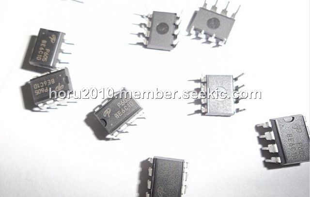
The AOP605 is a Complementary Enhancement Mode Field Effect Transistor. The AOP605 uses advanced trench technology to provide excellent RDS(ON) and low gate charge. The complementary MOSFET form a high-speed power inverter, suitable for a multitude of applications. The AOP605 is electrically identical.
Parametrics
AOP605 absolute maximum ratings: (1)Drain-Source Voltage: 30V for N-channel; -30V for P-channel; (2)Gate-Source Voltage: ±20V; (3)Continuous Drain Current TA=25℃: 7.5A; -6.6A; (4)Continuous Drain Current TA=70℃: 76A; -5.3A; (5)Pulsed Drain Current: 30A; -30A; (6)Power Dissipation TA=25℃: 2.5W; (7)Power Dissipation TA=70℃: 1.6W; (8)Junction and Storage Temperature Range: -55℃ to 150℃.
Features
AOP605 features: (1)VDS (V) = 30V for N-channel; -30V for P-channel; (2)ID = 7.5A (VGS = 10V); -6.6A (VGS = -10V); (3)RDS(ON); (4)<28mW (VGS = 10V); <35mW (VGS = -10V); (5)<43mW (VGS = 4.5V); <58mW (VGS = -4.5V).
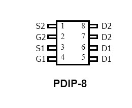
Diagrams
| Image | Part No | Mfg | Description |  |
Pricing (USD) |
Quantity | ||||
|---|---|---|---|---|---|---|---|---|---|---|
 |
 AOP605 |
|
MOSFET N/P-CH COMPL 30V 8-PDIP |
Data Sheet |
Negotiable |
|
||||
 |
AOP605L |
Other |
|
Data Sheet |
Negotiable |
|
||||